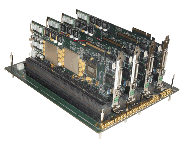
HES7XV4000BP – SoC/ASIC Prototyping and Emulation
HES7XV4000BP is a dual AMD Virtex 7 FPGA prototyping and emulation board for small and medium sized ASIC designs or large FPGA designs. The board provides a capacity of 24 Million ASIC gates estimated for 60% of FPGA utilization and is scalable up to 96 Million gates. There is one SO-DIMM slot for DDR3 memory connected to one of the Virtex 7 FPGA providing up to 8GB of external RAM to the emulated design. The highest quality PCB design with proper on-board trace routing assures reliable LVDS and GTX transfers up to the inherent limits of the FPGA device. A very precisely designed clocking block provides 5 length aligned global clock lines routed to each FPGA device. It also provides multiple configuration options due to integrating different oscillators, programmable clock synthesizers, and crosspoint switch multiplexers. The HES-7 prototyping solution was architected to provide easy implementation and expansion in a rack form factor with non-proprietary Backplane for flexible and scalable hardware configurations.
主要特性与优势
- Cost effective bundle with Aldec high performance simulators Active-HDL or Riviera-PRO
- Superior quality backed by industry leading 1-year warranty
- Rack form factor chassis for Backplane configurations
- Prototyping hardware reuse for acceleration and emulation verification modes
- Available in a scalable capacity up to 96 million ASIC gates
- 2x SATA
- PCIe x8 gen2
- USB 3.0 & 2.0
- BPX - non-proprietary backplane and daughter card connectors
- 5x global, low-skew, length-aligned clock lines and configurable clocking blocks
- DDR3 SO-DIMM up to 8 GB
- 1x Kintex 7 XC7K325T host FPGA
- 2x Virtex 7 XC7V2000T main FPGAs
包裝內容物含配件
- Diagnostic tests suite
- HES Proto-AXI software for board configuration and management
- HES-7-4000 board with 2 Xilinx® Virtex®-7 2000T FPGAs
- Optional HES-DVM software to enable Emulation and Simulation Acceleration
- Optional Proto-AXI interface, high speed PCIe to AMBA AXI bridge
- Reference designs for board interfaces
